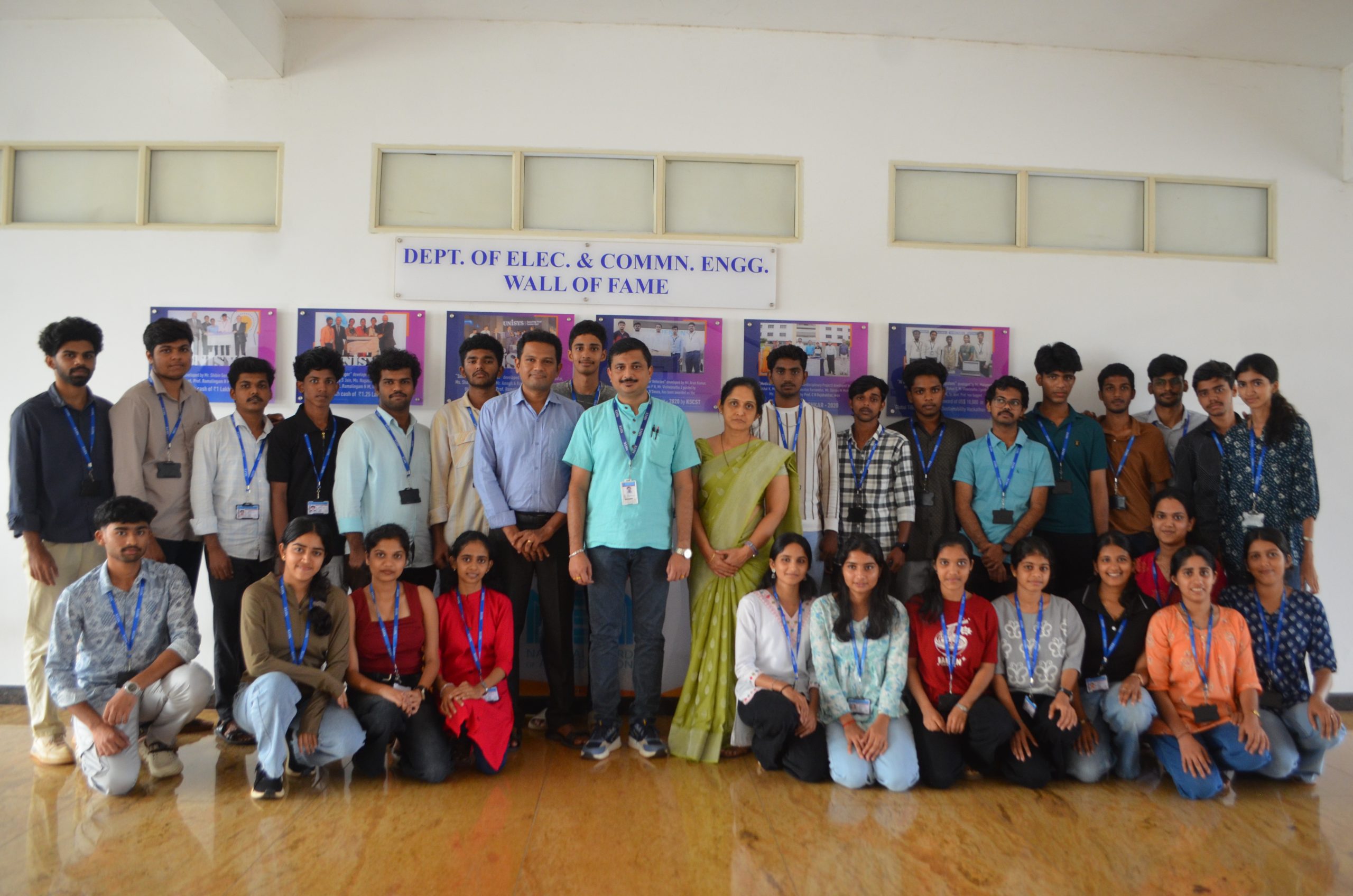
 The Department of Electronics & Communication Engineering, Mangalore Institute of Technology & Engineering (MITE), organized a three-day hands-on workshop on “From Circuits to Silicon: Exploring IC Design and Layout” from 12th to 14th November 2026, at the Embedded Systems/VLSI Laboratory. The workshop aimed to provide students with practical exposure to integrated circuit design, simulation, and physical layout methodologies while bridging the gap between theoretical knowledge and industry-oriented semiconductor design practices. The third-semester Electronics & Communication Engineering students actively participated in the workshop, gaining valuable hands-on experience in the complete IC design flow, from fundamental circuit analysis to verified CMOS layout.
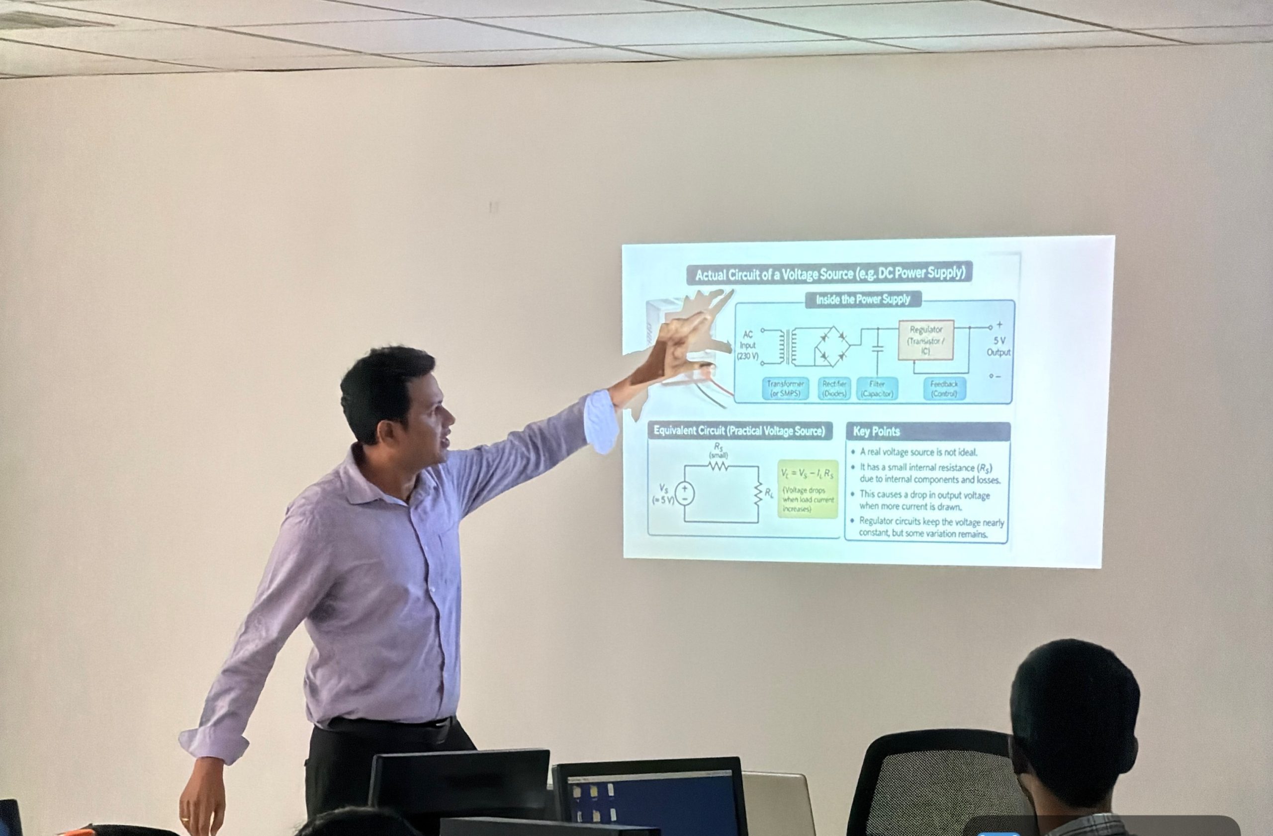
 The resource person for the workshop was Mr. Manjunath Shet, Founder and Lead Trainer, OCTAWAVE Technology, Mangalore, an organization specializing in skill development and industry-oriented training in VLSI design and semiconductor technologies. He has extensive experience in training engineering students and professionals in analog and digital IC design, circuit simulation, transistor-level design, RTL design and verification, and physical design, using both industry-standard and open-source Electronic Design Automation (EDA) tools. His strong practical expertise in semiconductor design and structured, hands-on teaching approach enabled participants to gain a comprehensive understanding of the design process, progressing from basic circuit concepts to complete IC layout development.
The workshop provided participants with a systematic understanding of the integrated circuit design flow, combining theoretical concepts with guided demonstrations and practical laboratory exercises. The initial sessions focused on circuit analysis and simulation using LTspice, where students analysed RC circuits and filters through DC, transient, and AC analysis and compared simulated responses with theoretical expectations. The sessions also reinforced fundamental semiconductor concepts, including PN junction behaviour, MOSFET operation, operating regions, and device characteristics, helping students establish a strong foundation for transistor-level circuit design.
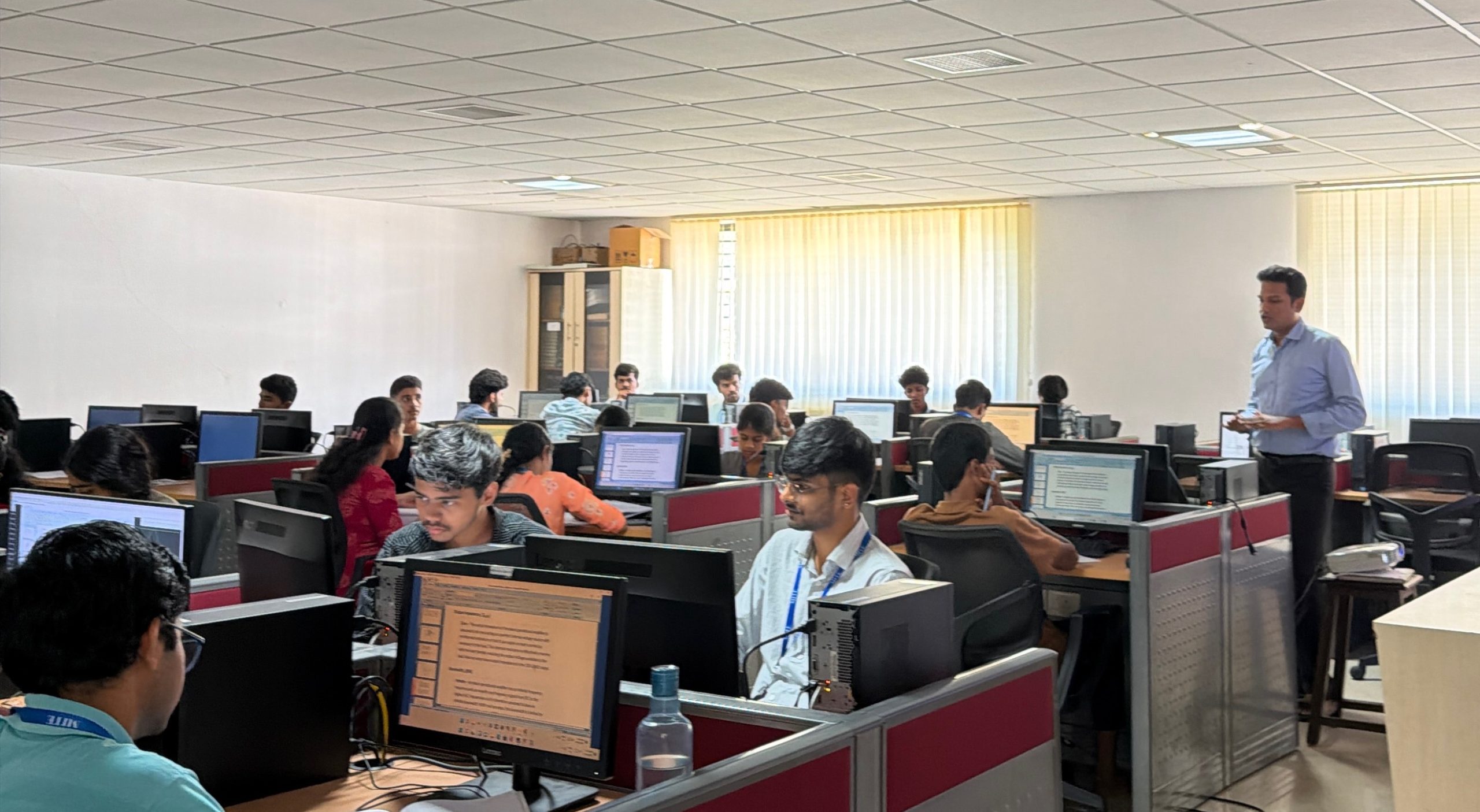
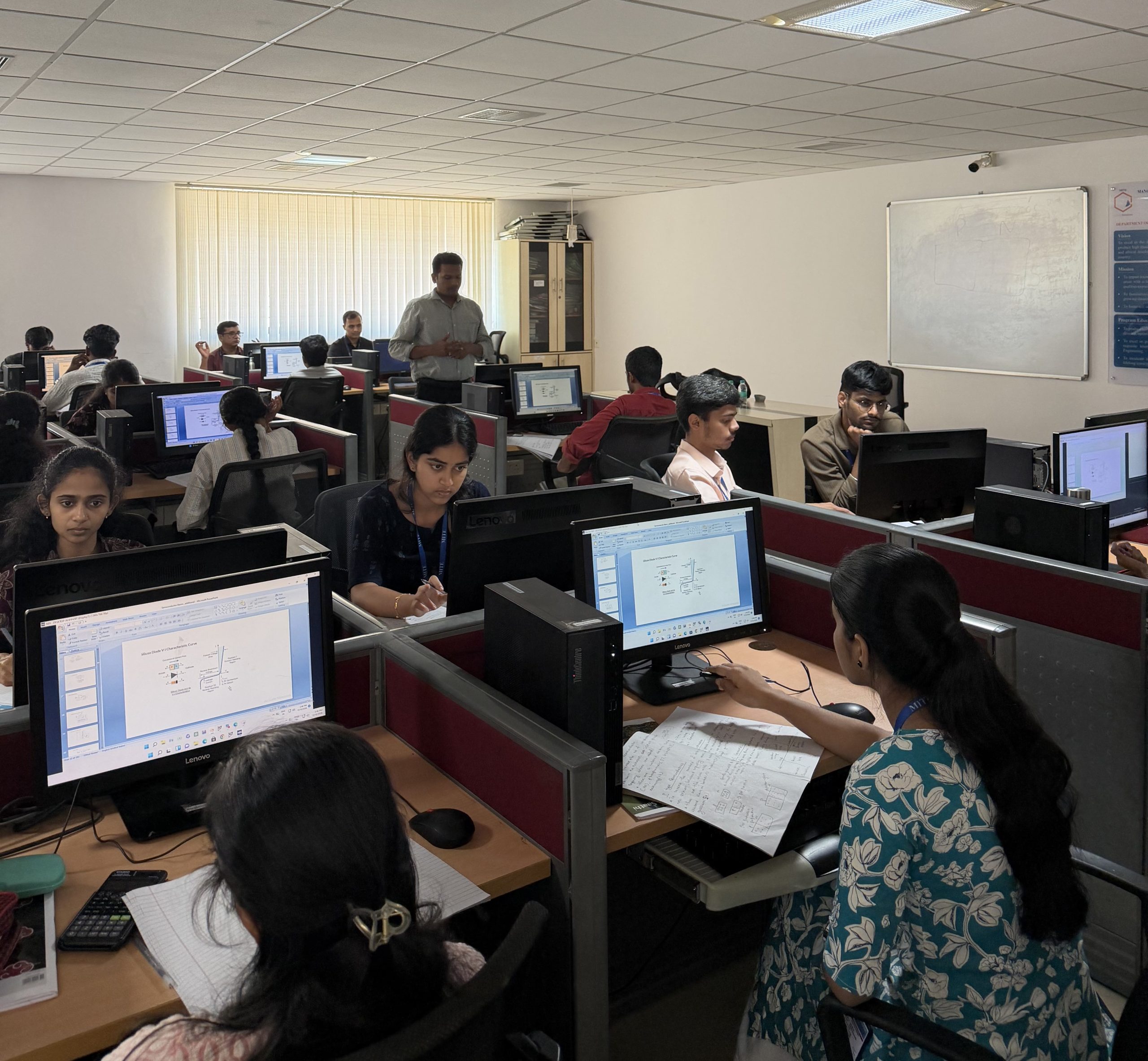 The subsequent sessions introduced students to Cadence Virtuoso, an industry-standard environment for custom IC design and simulation. Participants designed and simulated a CMOS inverter and a common-source amplifier at the transistor level, examining important circuit characteristics such as voltage transfer characteristics, noise margins, and propagation delays. Through hands-on exercises, each participant developed a CMOS inverter layout and performed Design Rule Check (DRC) and Layout Versus Schematic (LVS) verification, gaining practical exposure to the verification procedures followed in semiconductor design. These activities helped students understand the importance of design accuracy, layout constraints, and systematic verification in developing reliable integrated circuits.
The event was coordinated by Mr. Divyesh Divakar and Ms. Deepthi Kotian, Assistant Professors, Department of Electronics & Communication Engineering, MITE. The workshop concluded successfully with active participation and enthusiastic engagement from students. Overall, the programme served as an effective platform for experiential learning, strengthening technical competence, and enhancing industry readiness in the VLSI and semiconductor domains. By introducing third-semester students to the complete schematic-to-layout design cycle, the workshop encouraged early exploration of semiconductor technologies and supported the department’s commitment to developing industry-relevant VLSI design capabilities aligned with India’s growing semiconductor ecosystem.