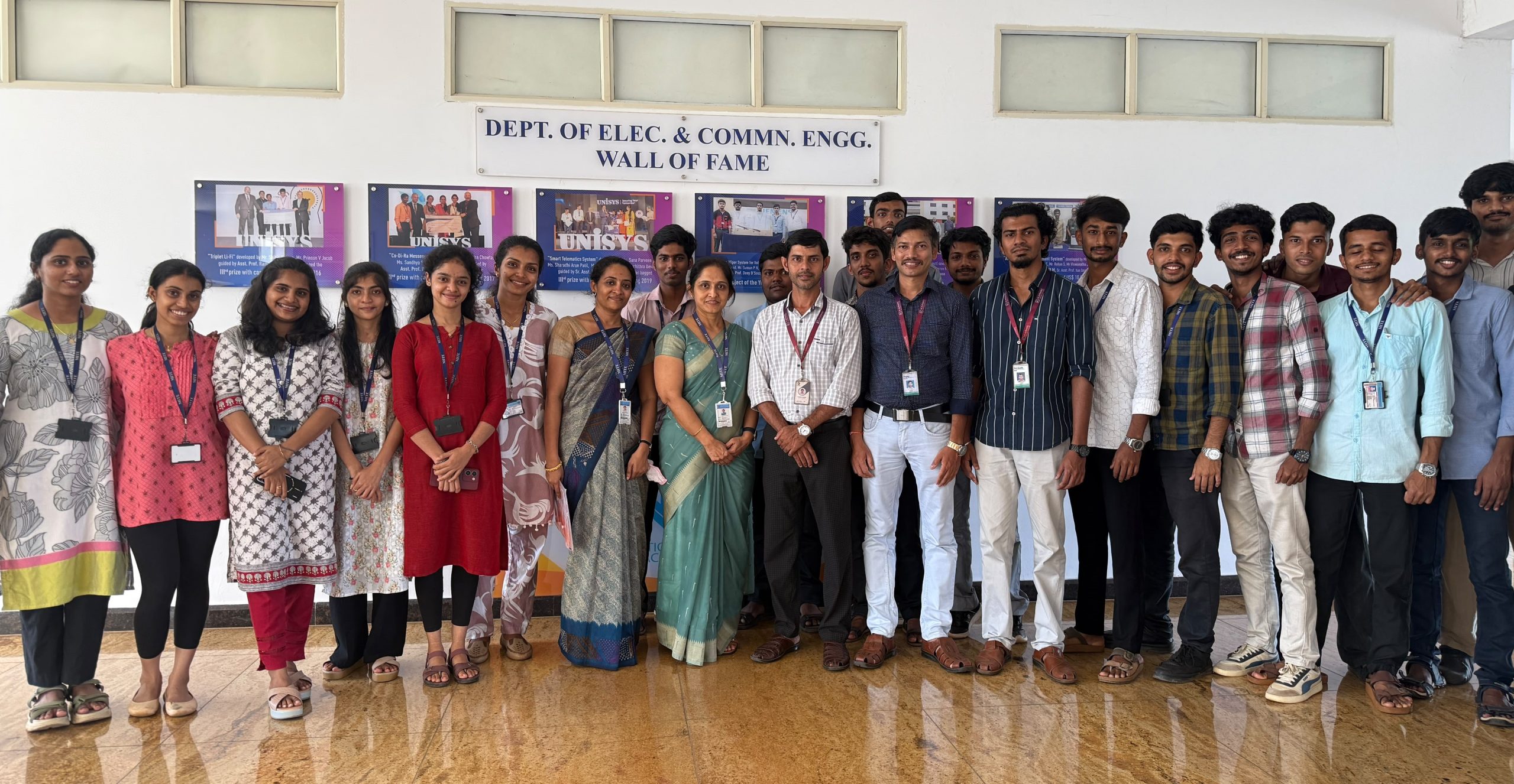
The Department of Electronics & Communication Engineering (ECE), Mangalore Institute of Technology & Engineering (MITE), in association with the Electronics & Communication Engineering Students’ Association (ECSA), organized a three-day workshop on “VLSI Layout Design: Leveraging Cadence Tools for Industry Applications” from 16th to 18th September 2026. The workshop was aimed at providing students with practical exposure to VLSI physical design and industry-oriented layout methodologies. A total of 26 students participated in the programme, gaining valuable hands-on experience in contemporary VLSI design practices.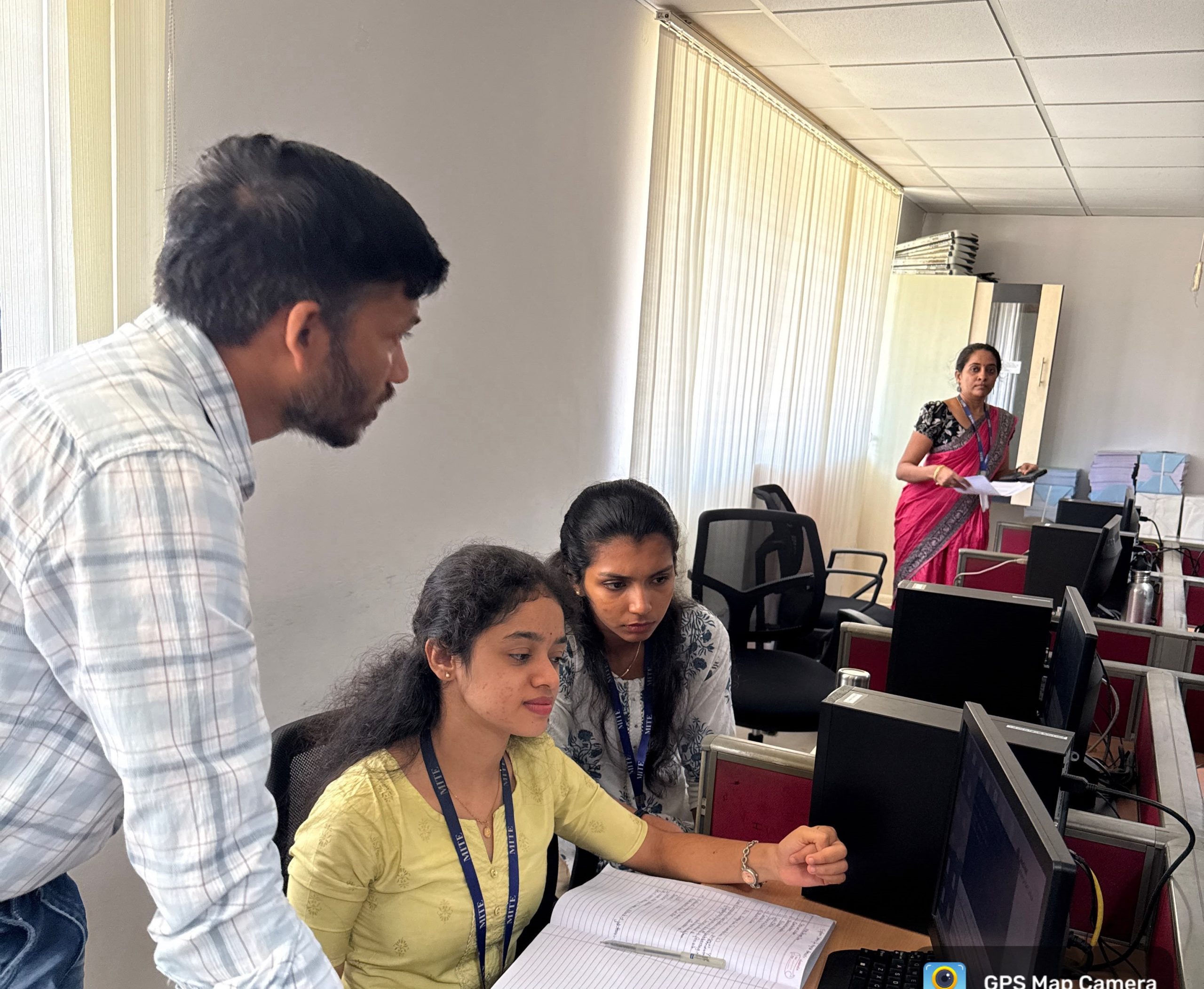
The resource persons for the workshop were Mr. Sujay Kumar, Principal Engineer, and Mr. Sandesh Kumar, Layout Design Engineer, KarMic Design Pvt. Ltd., Manipal. Mr. Sujay Kumar has over 16 years of industry experience and specializes in Analog and Mixed-Signal Layout Design. He has worked closely with Texas Instruments (TI) on modules and test chips involving power management and data converter blocks such as DC-DC converters, LDOs, ADCs, and DACs, and currently leads teams and projects in analog and mixed-signal layout design. Mr. Sandesh Kumar has over 3 years of industry experience in 28 nm, 45 nm, and 65 nm technology nodes, along with more than 12 years of teaching experience in VLSI and related areas. He has published and presented more than 20 research papers and has also conducted technical workshops under the Atal Tinkering Labs initiative, promoting innovation and hands-on learning. The workshop was supported by Mr. Sanketh C. Naik, Design Engineer–I.
The workshop provided students with practical exposure to MOSFET fabrication, ASIC design flow, and VLSI physical design using Cadence tools. The hands-on sessions covered N-type and P-type MOSFET layout, inverter layout, level shifter layout, and level shifter array design, enabling participants to understand the various stages involved in developing physical layouts for integrated circuits. Through practical exercises and expert demonstrations, students gained familiarity with industry-oriented design practices and developed a better understanding of the relationship between circuit design and physical implementation.
The event was organized under the guidance of Dr. Vinayambika S Bhat, HoD – E&CE, Dean – Quality Assurance, and coordinated by Ms. Deepthi Shetty, Senior Assistant Professor and Ms. Vimitha A, Assistant Professor, Dept. of E&CE. The workshop concluded on 18th September 2026 with student feedback and an interactive session with the resource persons. The experts shared valuable insights into VLSI career opportunities, placement preparation, industry expectations, and job opportunities in the semiconductor domain, providing students with a broader understanding of career pathways in the field. Overall, the workshop enhanced students’ practical skills, industry awareness, and understanding of contemporary VLSI layout design methodologies.