
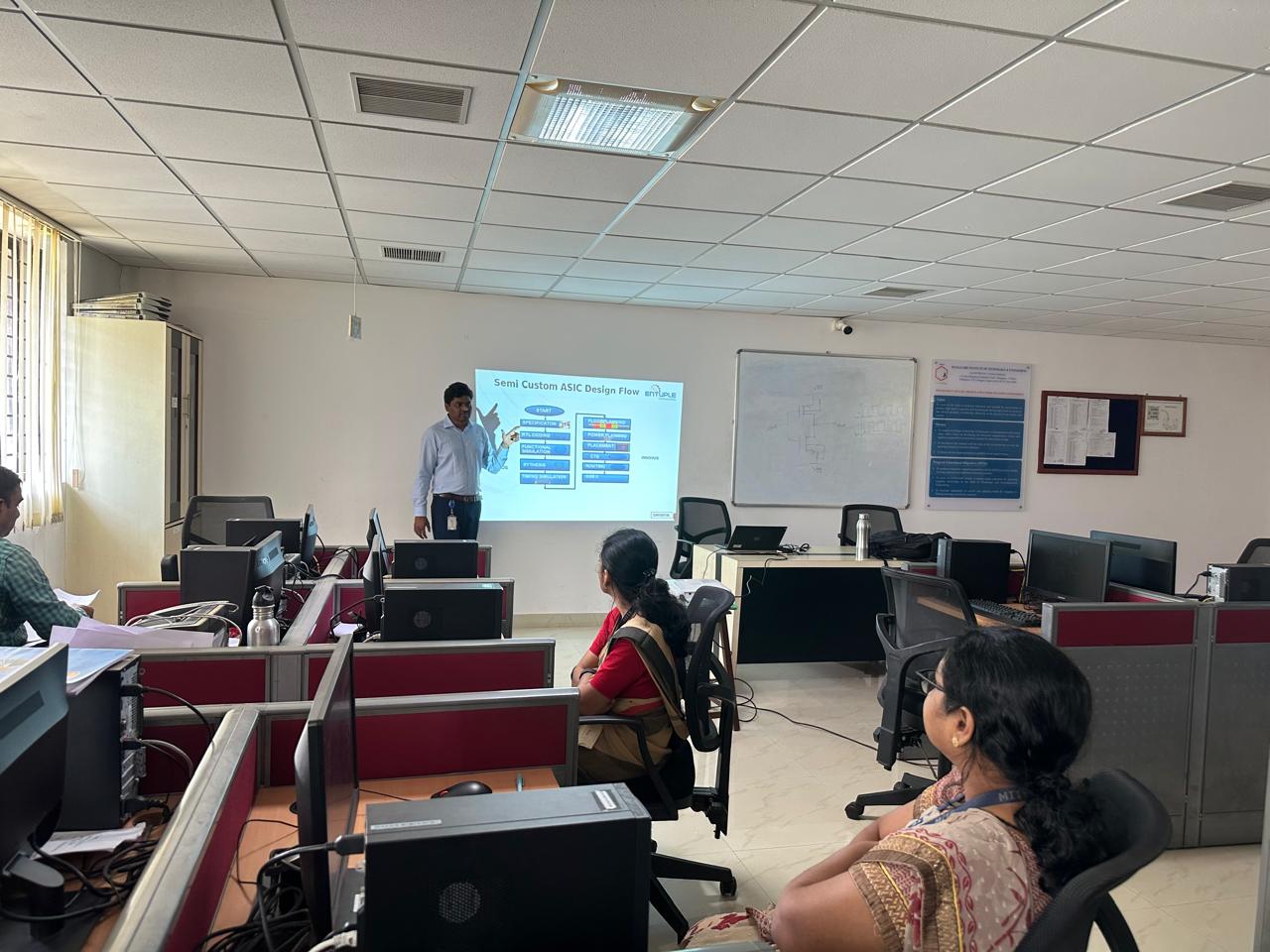
 The Department of Electronics & Communication Engineering, in association with IQAC-MITE, organized a three-day hands-on training session titled “From Ideation to Silicon: A Hands-on Custom IC Design with Cadence” from 2nd to 4th September 2025. The session was led by Mr. P. Rajendra, a Field Application Engineer at Entuple Technologies with over four years of experience in VLSI design. He began his career as a VLSI Application Engineer and is presently engaged in design and EDA support for industrial client projects and academic training. His expertise spans VLSI architecture, ASIC, FPGA, and SoC design.
 The workshop provided participants with practical exposure to the complete IC design process from schematic capture to silicon-ready layout. Topics included full custom design, semi-custom design, and analog mixed-signal flows. Participants gained experience in schematic design, testbench creation, simulation, layout design, verification (DRC & LVS), parasitic extraction, timing and power analysis, and GDSII generation using industry-standard Cadence EDA tools.
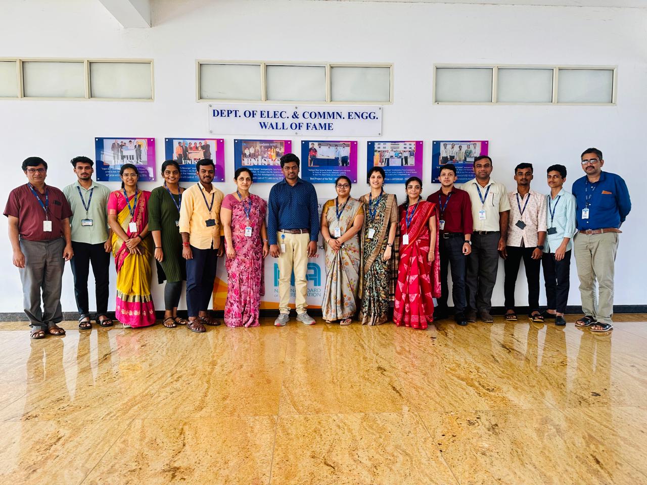
A total of 5 final-year students and 10 faculty members participated. The session successfully bridged the gap between theoretical concepts and real-world design practices, enhancing participants’ confidence in handling digital, analog, and mixed-signal circuits with professional methodologies.